|
Outline
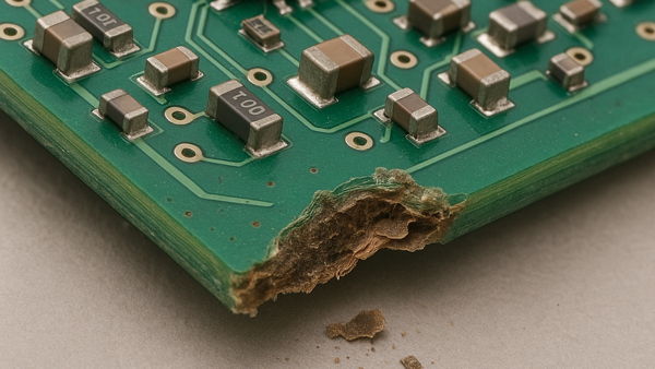
This procedure is used to repair minor damage to circuit base board material. Scrapes and scratches in the base board material may be caused by accidents during handling. Burns in the base material may be caused by improper use of soldering and desoldering tools.
|
||||||||||||||||||||||||||||||||||||||||||||
|
Procedure
Procedure
Evaluation
|
||||||||||||||||||||||||||||||||||||||||||||
Images and Figures
Base Material Repair, Epoxy Method
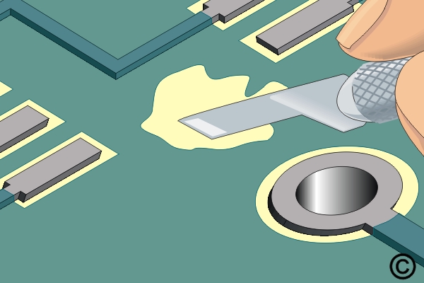
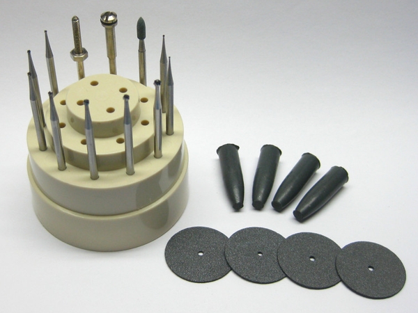
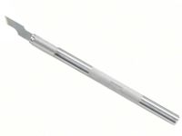
Figure 1. Scrape away damaged base board material with a knife.
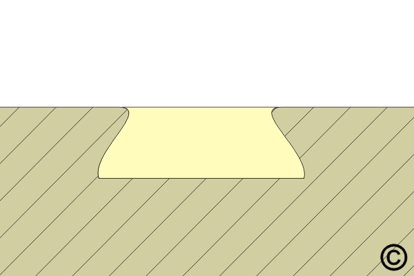
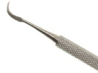
Figure 2. An undercut, to enhance mechanical strength, may be desired for class 3 product.
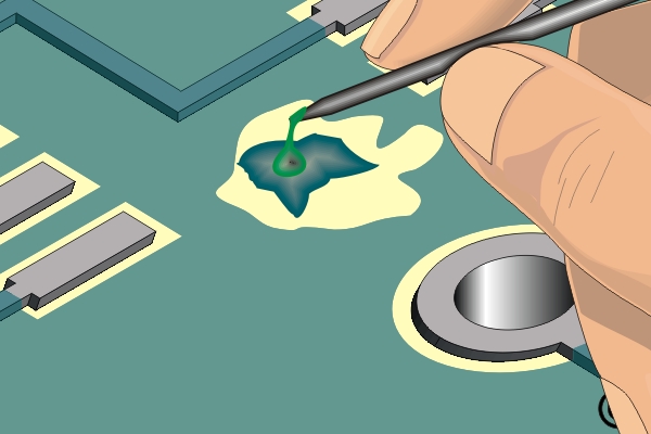
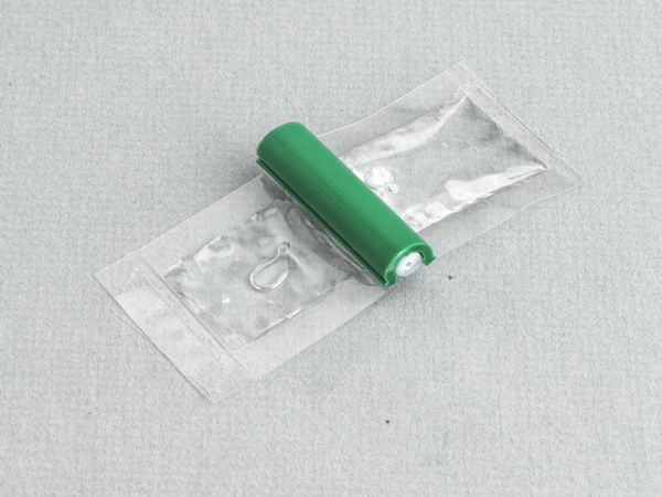
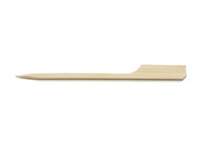
Figure 3. Apply the epoxy with a mixing stick sharpened at the end.

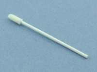
Figure 4. For large areas, apply the epoxy with a foam swab to create a texture.
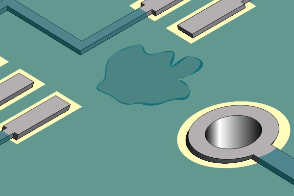
Figure 5. Completed repair.
|
||||||||||||||||||||||||||||||||||||||||||||
3.5.1 Base Material Repair, Epoxy Method
Procedure covers minor repair of damaged base board around edges on circuit board assemblies.
Minimum Skill Level: Advanced
Conformance Level: High
REQUEST FOR QUOTE GUIDES INDEX