Essential Practices for Gold Mitigation of Electronic Components
Introduction
This paper addresses the critical issue of gold mitigation in electric components. With a focus on the challenges gold poses in electronic assemblies, the paper explores various essential practices to effectively mitigate the use of gold. It discusses the importance of understanding the potential risks associated with gold, such as price fluctuations and environmental concerns, and provides strategies to minimize gold usage while maintaining high-quality performance.
The paper offers valuable insights and guidelines for manufacturers and engineers to navigate the complexities of gold mitigation in electronic component manufacturing and design.
Details
Since gold plating dissolves rapidly during the soldering process, the remaining gold within a solder joint can weaken the integrity of the interconnection. If this gold dissolution is excessive during the solder alloy’s liquidus phase formation, the composition and mechanical properties of the resulting solder joint will change.
Gold embrittlement within tin-lead (SnPb) solder joints is a well-known failure mechanism. Commonly used lead-free solder alloys, including tin-silver-copper (SAC305) and tin-nickel-copper (SN100C), are more capable of maintaining their mechanical properties when combined with gold partially due to the greater tin content. However, lead-free solder joints will also degrade with increased gold inclusion.
Gold embrittlement can be a significant reliability issue, with the risk of embrittlement dependent upon several variables, including the amount of gold expected to be leached from the plated surfaces, the volume of the resulting solder joint, and whether the solder is from an infinite source such as a wave or selective soldering process, or reflowed solder paste. In most cases, excessive gold dissolution is from gold-plated component leads rather than the gold contribution from the printed circuit board finish, such as electroless nickel immersion gold (ENIG) or electroless nickel electroless palladium immersion gold (ENIPIG). These board finishes are typically too thin to contribute to gold embrittlement since their average thickness is below the threshold considered a minimal contribution to gold embrittlement.
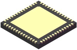
1. QFN component with gold plated surfaces.
Removal of gold plating from component leads is typically performed by a pre-tinning process which removes the gold as it is solubilized in the molten solder during a component re-tinning process. A double tinning process in a static solder pot or single tinning process in a dynamic solder wave should be used for gold removal before soldering the components into a board assembly, as improper removal of gold on component leads and terminations before board-level assembly can potentially result in solder cracks and/or field failures.
Beginning with the IPC J-STD-001 Rev F requirements implemented in 2014 and continuing to the current Rev H requirements, it is stated that gold shall be removed from all Class 2 and Class 3 products for the following conditions:
At least 95% of the surfaces to be soldered of through-hole component leads with 2.54µm or more gold thickness.
From 95% of all surfaces to be soldered of surface mount components regardless of gold thickness.
From the surfaces of solder terminals plated with 2.54µm or more gold thickness.
With this criterion, gold removal is required for all high-reliability Class 2 and Class 3 electronic products and affects almost everyone in the electronics manufacturing industry; gold removal is no longer limited solely to aerospace and military applications.
The ideal method to facilitate the removal of gold plating from SMT and through-hole components is to use the robotic hot solder dipping (RHSD) process. It is recommended that this re-tinning operation be carried out using a lead tinning machine using controlled flux application, preheating, single or dual solder pots, nitrogen inerting, and defined process control. A defined process of this type is highly recommended instead of manually dipping components into a standalone static solder pot to reduce solder contamination, minimize non-wetting issues, and enhance solderability.
2. Robotic hot solder dip systems for tinning and gold mitigation.
Robotic hot solder dip (RHSD) machines can use single or dual static or dynamic solder pots. When dual static pots are used, the first pot removes gold plating, oxidation, or other residues, and the second pot is used for precise control over solder depth. A nitrogen-inert atmosphere helps the appearance of the resulting solder finish while mitigating icicles and dross buildup. Immersion of the component leads or terminations into the flux and solder should be controlled to allow the flux and solder to flow up the lead or termination to a controlled depth. A defined withdrawal or extraction speed should be used in the second solder pot to control the re-tinning solder thickness and solder pots should be tested regularly for copper, nickel, and other contaminants.
Using a fully programmable robotic hot solder dip (RHSD), machine is highly recommended as opposed to manual solder dipping since these robotic systems precisely control the solder dip depth, dwell times, preheat, and solder temperatures in full compliance with GEIA-STD-0006 standards. The GEIA-STD-0006 standard, Requirements for Using Solder Dip to Replace the Finish on Electronic Piece Parts, states that robotic solder dipping apparatus shall have:
Dynamic solder wave or other method to remove oxidation before solder dipping.
Controlled dwell time in preheat and solder pot within ± 0.1 sec.
Controlled depth of immersion to within ± 0.1mm.
Controlled exit speed from solder pot to within ± 0.3 cm/sec.
Piece parts shall be pre-heated to no less than 71°C before solder dipping.
Total immersion time shall be less than 5 seconds on each component side.
Robotic hot solder dip tinning services can remove gold plating from through-hole, and SMT component leads or pads to minimize the risk of gold embrittlement as a potential failure mechanism. When these robotic hot solder dip tinning services, it is recommended to also use a batch wash system for post-process cleaning as well as the following procedures:
Component moisture sensitivity level (MSL) dry bake per J-STD-033.
Component moisture sensitivity level (MSL) packaging per J-STD-020.
Tape and reel packaging per EIA-481.
Tray packaging per JEDEC95.
If available from your robotic hot solder dip tinning service provider, the following testing services are beneficial and recommended to ensure process integrity:
Ionic cleanliness (ROSE) testing per IPC-TM-650-2.3.25.
X-ray fluorescence (XRF) for alloy composition and finish thickness per ASTM B568, JESD 213.
Solderability testing per J-STD-002.
Visual inspection per JESD22-B101.
For ultra-high reliability, mission-critical applications such as military, security, defense, and/or aerospace, additional component testing services can be required utilizing the following test protocols:
Pre and post-processing acoustic microscopy testing (CSAM) per MIL-STD-1580.
Destructive physical analysis (DPA) per EIA-595 or EIA-469.
Hermeticity testing (fine and gross leak) per MIL-STD-883, method 1014, MIL-STD-750 method 1071, MIL-STD-202, method 112.
Temperature, humidity, and bias testing.
Parametric testing.
Conclusions
This paper sheds light on the crucial issue of gold mitigation in electric components. The paper highlights the potential environmental and economic benefits of reducing gold usage by emphasizing the significance of gold mitigation in electronics manufacturing. The paper explores various practices and techniques and provides valuable insights into effective strategies for mitigating gold in electronic components.
As the demand for electronics continues to rise, implementing these essential practices promotes sustainability and contributes to the optimization of manufacturing processes and cost reduction. Overall, this paper serves as a comprehensive guide for industry professionals and researchers, paving the way for responsible and efficient gold mitigation practices in the electronics sector.
Several members of the Circuit Technology Center team contributed to this feature story.